
Receiver
For maximum linearity of response, the MWA will use a direct RF sampling receiver architecture. The receiver consists of all components between the RF output of the analog antenna tile beamformer, and a high spectral resolution (8 kHz) digital data stream transmitted to the central processing facility. In this case, the "F" part of the "FX" correlator architecture becomes part of the receiver.
The receiver consists of two parts. The front end is a small analog & mixed-signal board consisting of a single fixed low-pass and sky-noise equalization filter, final amplifier, and fast A/D converter sampling RF in the 1st Nyquist zone (the 6-bit Maxim MAX105 and the 8-bit National ADC081000 are currently under evaluation and testing). The back end is a purely digital part implementing coarse spectral filtering, decimation to a selected 32 MHz subset, final spectral filtering to 4K channels of 8 kHz resolution, and aggregation of signals for fiber transport to the central processing facility.
The Receiver System
The receiver system will accept the RF data stream from 8 antenna tiles on coaxial cable and will output digital data stream on optical fiber. It will digitize the input RF signal after appropriate signal conditioning and pass the digitized stream through a coarse polyphase filter to obtain about a MHz wide channels. Nominally about 32 MHz of bandwidth per antenna will be selected for transmission. Each receiver ‘node’ enclosure will contain sufficient Monitor & Control and receiver related hardware to service 8 antenna tiles.
The 16 RF signals from eight analog beamformers enter the node enclosure through coaxial cables. They are fed to a Signal Conditioning Board to limit the bandwidth and adjust the power levels to suit the range of the digitizers. The Analog-to-Digital converters will be clocked at fs ~660 MHz. The digital data is fed to FPGA hardware in which a coarse polyphase filter bank is implemented to select 24 sub-bands yielding a total of 32 MHz bandwidth coverage from the full antenna tile bandwidth of 80-300 MHz. The digitized data is aggregated and reformatted for transmission via optic fibre to the correlator.
The node will contain additional components, including (a) Monitor & Control (m&c) capability to control the digital and analog hardware, relay and monitor beam-steering commands, and monitor environment and system health, (b) sampling clock module, and (c) possible driver electronics for synchronous phase-switching. The node enclosure will be weather tight, protected against lightning and RFI tight to avoid significant spurious emissions.
The principal components associated with the receiver node are shown in the schematic in Figure 1, and Figure 2 shows a schematic of the receiver monitor and control subsystem.
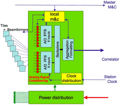
Figure 1. The principal components at the Receiver Node.
Copyright © 2009 Murchison Widefield Array. All rights reserved. | MWAinfo@MWAtelescope.org
